Circuit board production and processing process
-
open material
-
inner layer dry film
Plasma cleaning
-
browning
Plasma cleaning
-
laminated
-
drilling Plasma cleaning
-
Immersion copper plate plating
-
Outer layer dry film
Plasma cleaning
-
Outer graphic plating
-
Solder mask
-
Final inspection, random testing, packaging
-
Electrical test
-
molding
-
surface treatment
-
Silkscreen characters
Plasma cleaning
PCB inner layer dry film plasma cleaning
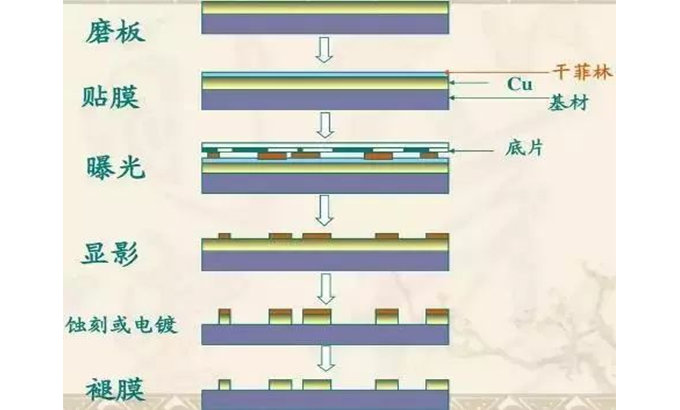
The inner layer dry film is the process of transferring the inner layer circuit pattern to the PCB board. The inner layer dry film includes multiple processes such as inner layer filming, exposure and development, and inner layer etching. The inner film is to paste a special photosensitive film on the surface of the copper plate, which is what we call dry film. The film cures when exposed to light, forming a protective film on the board. Exposure and development is to expose the board with the film attached, the light-transmitting part is cured, and the non-light-transmitting part is still a dry film. After developing, the uncured dry film is removed, and the board with the cured protective film is etched. After the film removal process, the circuit pattern of the inner layer is transferred to the board. The whole process flow is shown in the figure below.
1Expose
Align the negative film with the substrate on which the dry film has been pressed, and transfer the pattern of the negative film to the photosensitive dry film by irradiating with ultraviolet light on the exposure machine.
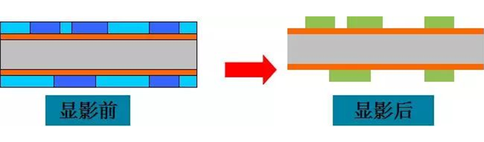
2development
Use the weak alkaline of the developer (sodium carbonate) to dissolve and wash away the unexposed dry/wet film, and the exposed part remains.
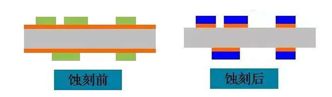
3Etching
After the unexposed dry film/wet film is removed by the developer, the copper surface will be exposed, and the exposed copper surface will be dissolved and corroded with acid copper chloride to obtain the desired circuit.
At present, the acid cupric chloride etching solution of cupric chloride and hydrochloric acid, and the alkaline cupric chloride etching solution of cupric chloride and ammonia water are the mainstream. The equipment is a horizontal conveying spray type, which can achieve maximum production automation and reduce costs, but this method is not perfect, and will lead to "pool effect", which will make the etching results different. Ordinary boards have little effect, but for ultra-fine lines, the tolerance requirements of etching cannot be met.
What happens when the "pool effect" occurs: when the PCB is transferred horizontally, it is located under the board and on the top of the board near the edge, the etching solution is easy to flow away, and the old and new etching solutions are easier to exchange; while the position in the center of the board is easy to form a "pool", etching Fluid flow is restricted; therefore, lines in the middle above the PCB will be less etched than elsewhere. Vacuum plasma has great advantages in the uniformity of treatment, and it is more effective for the treatment of soft boards and hard boards with smaller wire diameters, and there is no waste liquid treatment.
4 Demembrane
The exposed dry film protecting the copper surface is peeled off with sodium hydroxide solution to expose the circuit pattern.