


Please submit your message online and we will contact you as soon as possible!
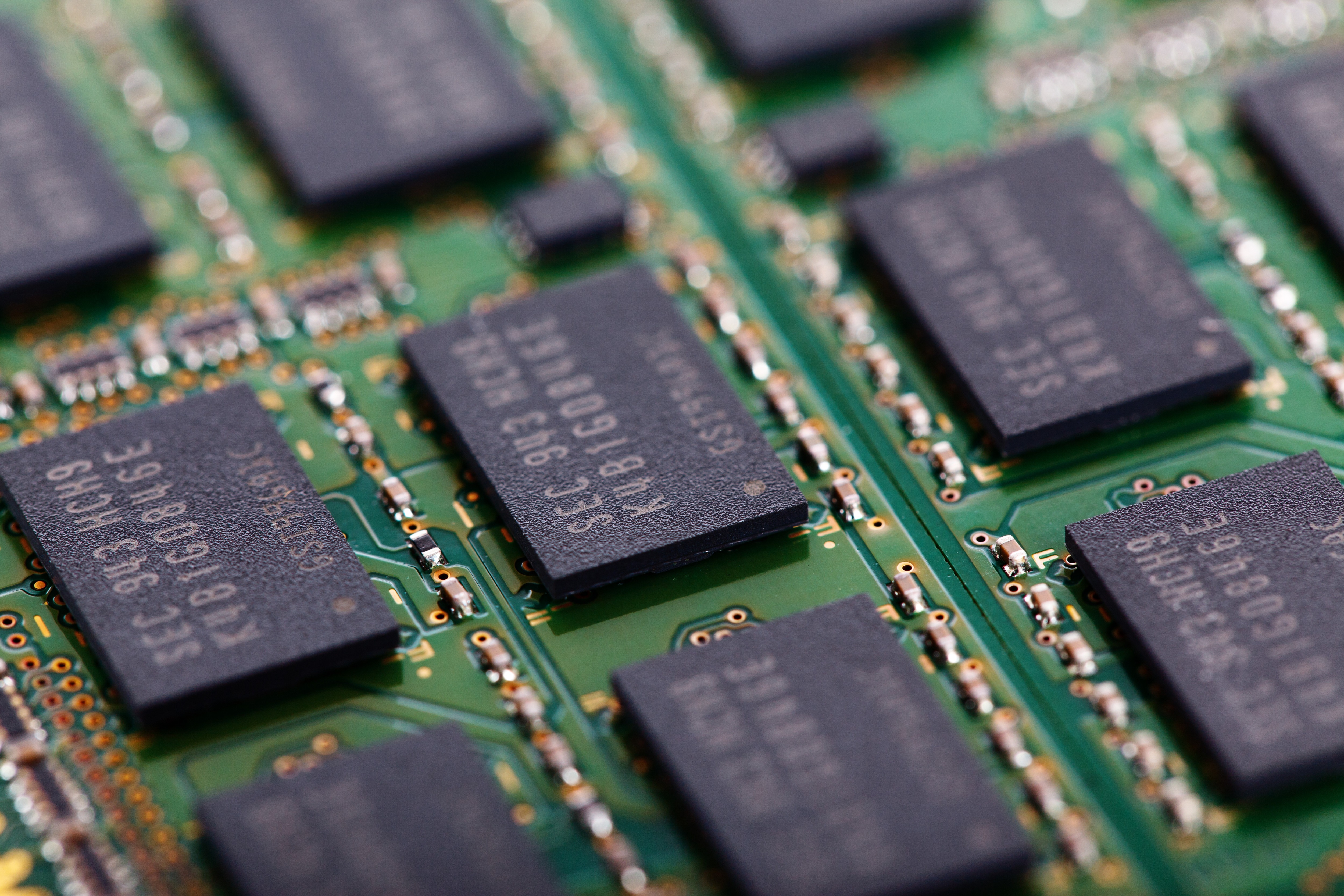
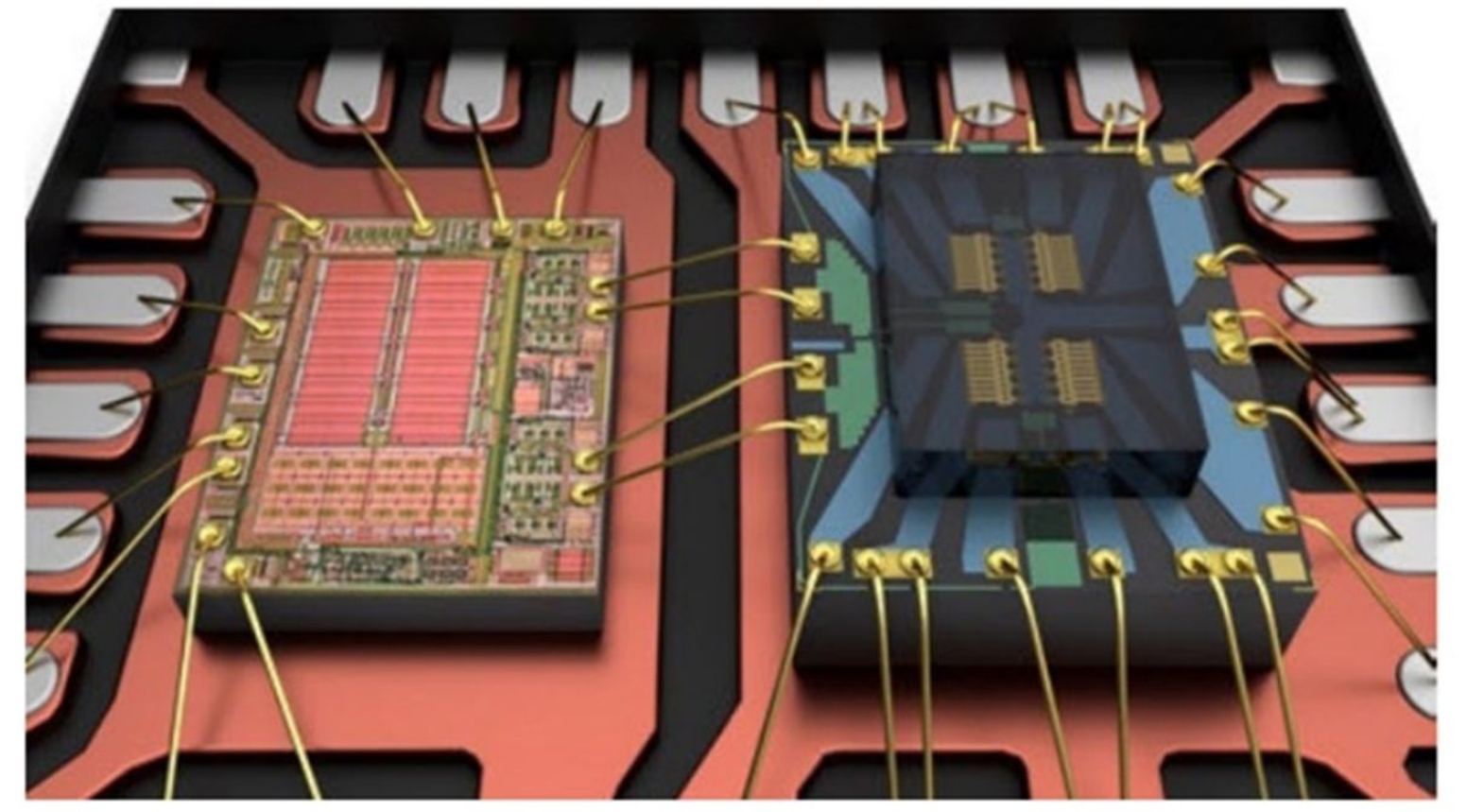
In the semiconductor packaging process, organic pollutants, oxide layers and other pollutants on the surface of the substrate, bracket and other accessories need to be surface treated, otherwise it will affect the yield of the entire chip packaging. Therefore, in order to ensure the quality of the entire process and products, microwave plasma cleaning equipment is usually introduced for plasma surface treatment to solve the above problems in the four process links of chip bonding, plastic sealing, photoresist removal, and metal bonding.
Remove contaminants on the surface of materials, increase surface wettability, improve colloid fluidity, and ensure binding ability with other materials.
Remove residual photoresist and other organics, activate and roughen wafer surface, and improve wafer surface wettability.
Removes organic contamination from metal pads, improving the strength and reliability of the soldering process.


Please submit your message online and we will contact you as soon as possible!