


Leading by innovation丨Win-win cooperation丨Building the chip manufacturing industry chain
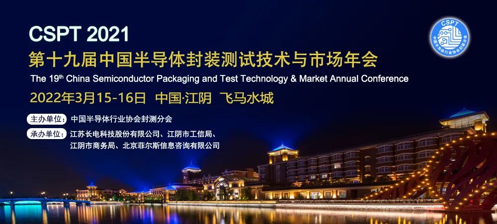
The 19th China Semiconductor Packaging and Testing Technology and Market Annual Conference
Exhibitor: Dongguan Sindin Precision Instrument Co., Ltd. Booth: No. 17
About Semiconductor Packaging and Testing Annual Conference
At present, the international situation is complicated and the integrated circuit industry, as a national strategic industry, has ushered in a critical period of development under the influence of the international situation. Innovation, openness, greenness, and integration are the development directions of the IC industry, and IC packaging and testing is an important link in the industry chain, and will also usher in major development opportunities and challenges.
With the theme of "innovation leadership, win-win cooperation, and joint construction of the chip manufacturing industry chain", the conference discussed hot issues in the industry such as innovation and trends in chip manufacturing, packaging and testing and equipment, and key materials.
About Sindin
Sindin is a national high-tech enterprise integrating R&D, design, production, sales and industrial chain services. Established a joint laboratory of plasma technology with South China University of Technology, and has more than 30 patented technologies and 10 senior technical experts in the industry.
Sindin Precision has been deeply engaged in the fields of material surface, electrical and electronic, industrial automation, etc., and is committed to providing professional surface treatment and testing overall solutions for global users.
This exhibition will bring a variety of microwave plasma cleaners, SPE series wafer plasma degumming machines and contact angle measuring instruments to booth 17. We sincerely invite you to gather together!
Star Products
①SPE series wafer plasma debonding machine: Remote plasma source provides excellent wafer processing solution with efficient photoresist stripping rate.
②SPMV-100H cavity microwave vacuum plasma cleaning machine: It is an overall solution for PLASMA processing and performance testing involved in the semiconductor industry.
③SDC-580 automatic wafer contact angle measuring instrument: specially designed for wafer wafer customers, the wafer contact angle testing equipment can meet the multi-point testing of 6-12 inch wafer samples at the same time.

