In the LED industry chain, the upstream is the epitaxial manufacturing and chip manufacturing of LED luminescent materials, the midstream is the LED device packaging industry, and the downstream is the industry formed after the application of LED display or lighting devices. The development of packaging technology with low thermal resistance, excellent optical properties and high reliability is the only way for new LEDs to become practical and market.
Packaging is the link between the industry and the market. Only after packaging can it become a terminal product and put into practical application.
.png)
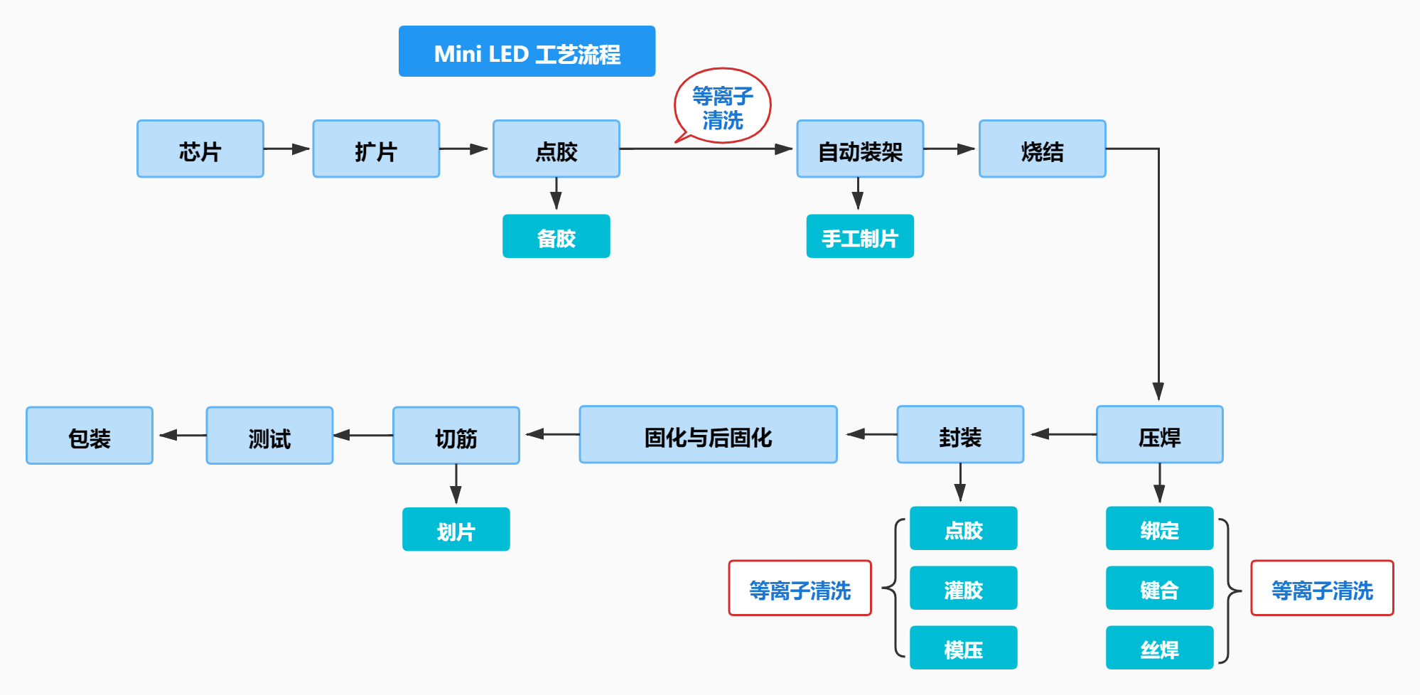
During the Mini LED packaging process, if there are particulate pollutants, oxides and epoxy resin pollutants on the chip and the substrate, it will directly affect the yield of Mini LED products. Before dispensing and wire bonding in the packaging process Plasma cleaning prior to encapsulation and curing can effectively remove these contaminants.
Mini LED packaging process
Plasma cleaning principle:
The surface of the object is treated by chemical or physical action to achieve the removal of pollutants at the molecular level (generally a thickness of 3-30mm), thereby improving the surface activity of the object. The removed contaminants may be organics, epoxy, photoresist, oxides, particulate contamination, etc. Corresponding to different pollutants, different cleaning processes should be used. According to the different process gases selected, plasma cleaning is divided into:
Chemical cleaning:The surface reaction is mainly plasma cleaning with chemical reaction, also known as PE.
Physical cleaning:Plasma cleaning in which the surface reaction is dominated by physical reactions is also called sputter etching (SPE).
Physical and chemical cleaning:Both physical and chemical reactions play an important role in surface reactions.
Application of plasma cleaning in Mini LED packaging process
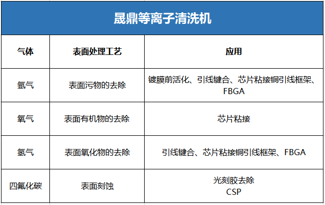
In the Mini LED packaging process, different cleaning processes can be used to achieve ideal results for different pollutants and different substrate and chip materials. However, using the wrong process gas solution will lead to poor cleaning results or even product scrap. For example, if the silver material chip adopts the oxygen plasma process, it will be oxidized and blackened or even scrapped. In general, the particulate pollutants and oxides are cleaned by plasma with a mixture of hydrogen and argon. The gold-plated material chip can use oxygen plasma to remove organic matter, but the silver material chip cannot. Choosing a suitable plasma cleaning process can be roughly divided into the following three aspects in Mini LED packaging:
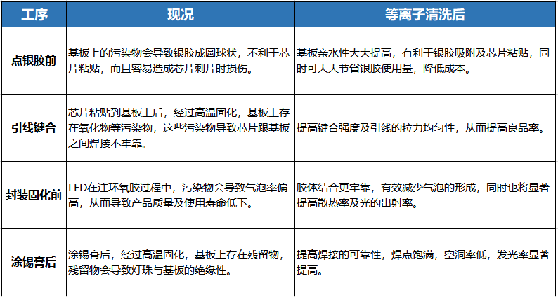
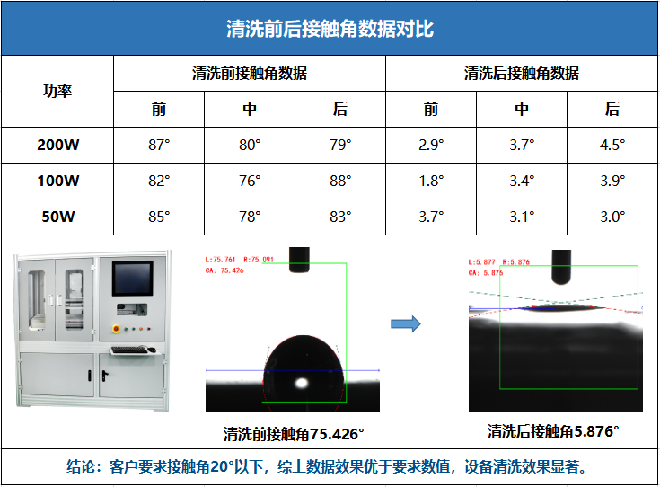
By comparing the contact angle data before and after plasma cleaning, it can be seen that the surface activation of the material, the removal of oxides and micro-particle pollutants, can be directly expressed by the tensile strength and wettability of the bonding wire.
Sindin plasma cleaning machine
The choice of plasma cleaning in the packaging process depends on the requirements of the subsequent process on the material surface, the characteristics of the material surface, the chemical composition, and the nature of the contaminants. Plasma cleaners can enhance the adhesion, wettability and reliability of samples, etc. Different processes use different gases.
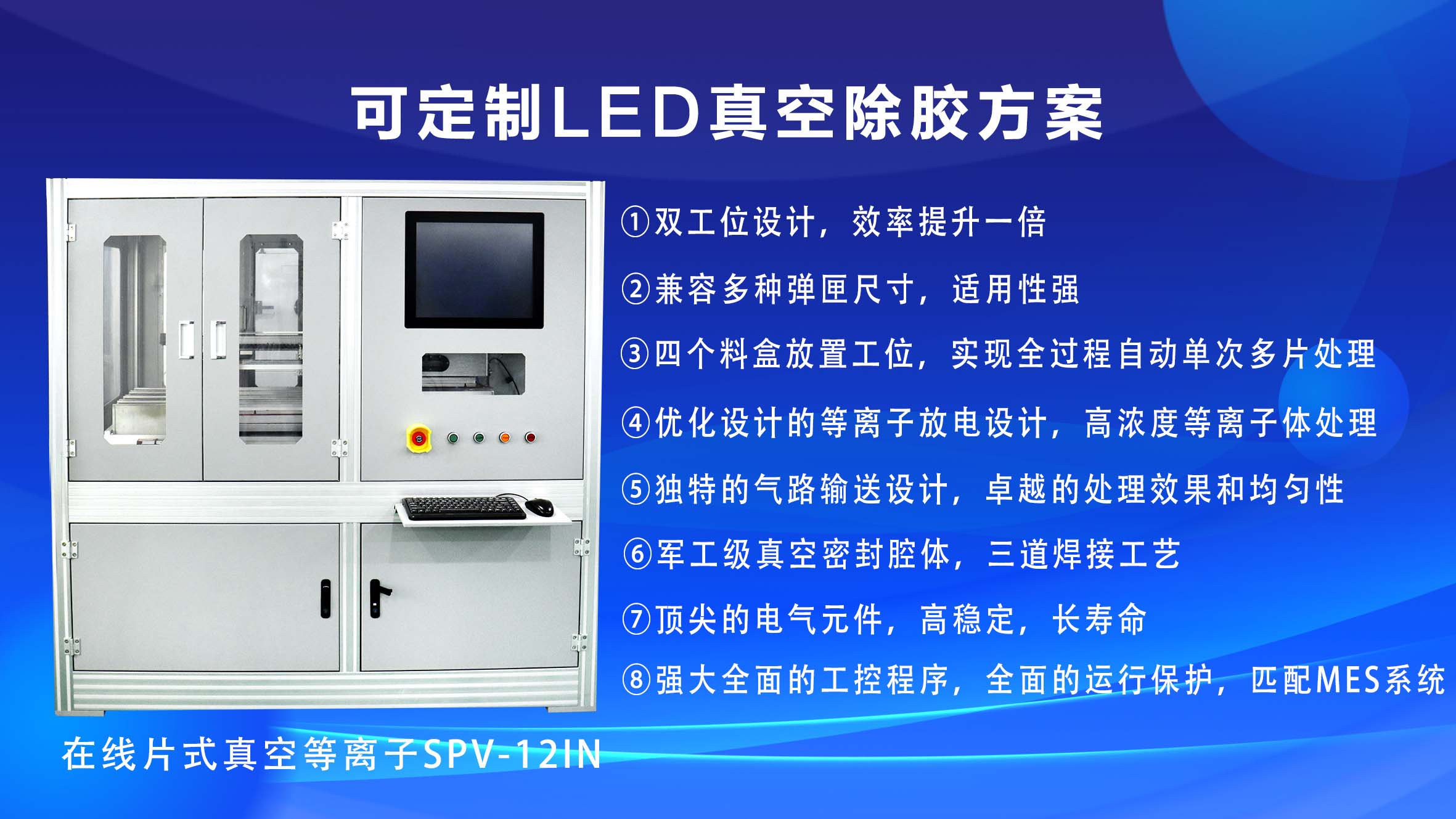
In-Line Vacuum Plasma Cleaner SPV-12IN
