Chip Packaging Technology
Chip packaging technology covers a wide range of technologies and belongs to complex system engineering. It involves various disciplines such as physics, chemistry, chemical industry, materials, machinery, electrical and automation, and also uses various materials such as metals, ceramics, glass, polymers, etc., so chip packaging is an interdisciplinary knowledge integration. Science, engineering technology that integrates factors such as electrical characteristics, thermal conduction characteristics, reliability, application of materials and process technology, and cost and price of products to achieve optimization purposes.
Packaging Engineering·Technical Level
The first level: chip-level packaging: the process of pasting and fixing the integrated circuit chip and the packaging substrate or lead frame, circuit wiring and packaging protection, making it easy to pick and place, and can be assembled with the next level. connected module elements.
The second level: the process of forming a circuit card with several packages completed in the first level and other electronic components.
The third level: the process of combining several circuit cards completed at the second level on a main circuit board to make it a component or subsystem.
The fourth level: the process of assembling several subsystems into a complete electronic product.
Implement the function
①Transfer function ②Transmit circuit signal ③Provide heat dissipation path ④Structural protection and support
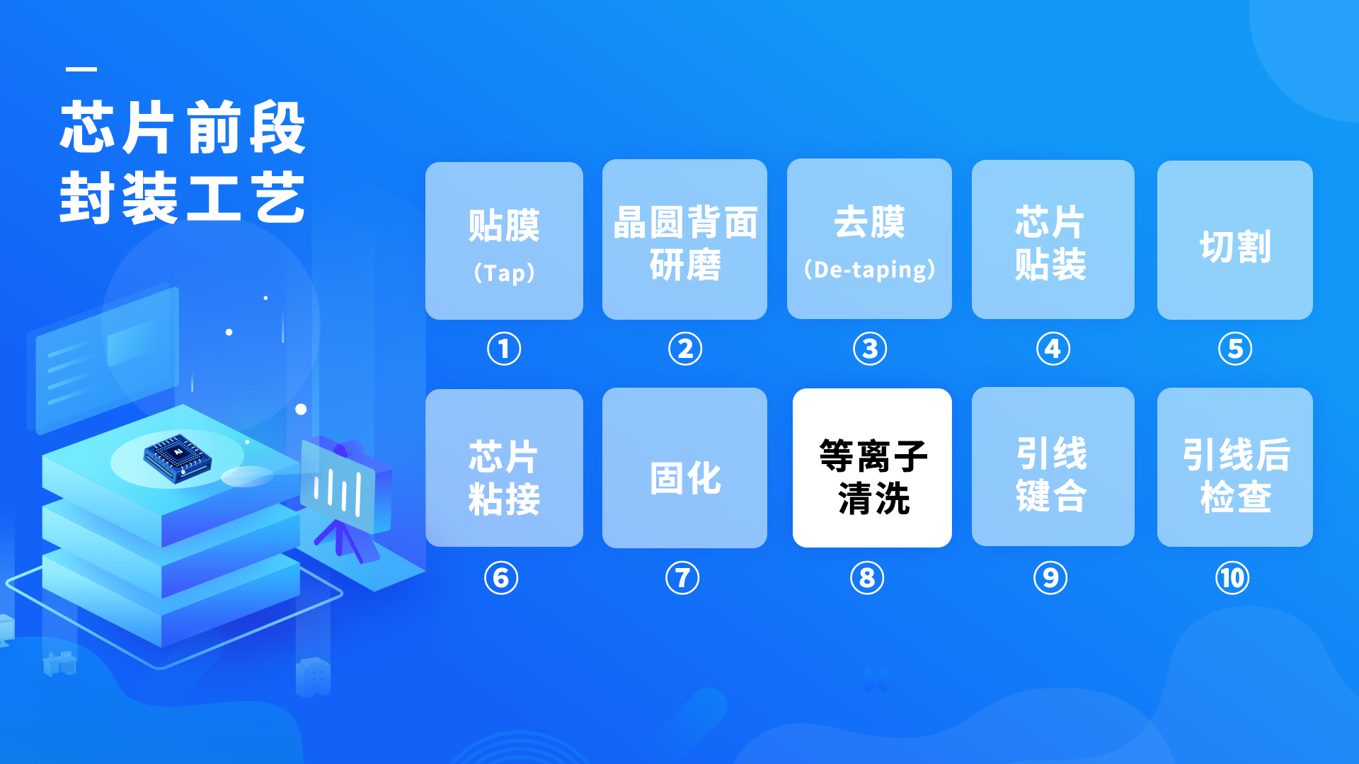
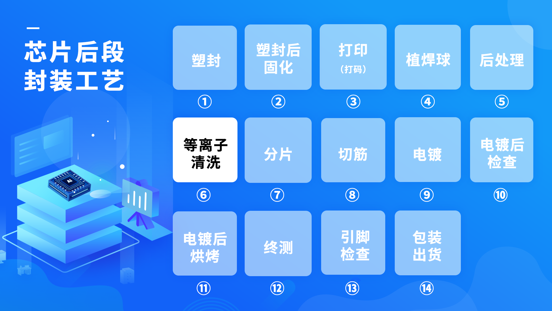
Front and rear encapsulation process

In the manufacturing process of hybrid integrated circuits, one of the main reasons for circuit failure is bonding failure. According to statistics, more than 70% of the product failures of hybrid integrated circuits are caused by bonding failures. This is because the bonding area will inevitably be polluted by various kinds of organic and inorganic residues during the production process, including various organic and inorganic residues. Processing and direct bonding will cause defects such as virtual soldering, de-soldering, low bonding strength and large differences in bonding stress, resulting in no guarantee of long-term reliability of the product. Plasma cleaning technology can effectively remove The pollutants in the bonding area can improve the surface chemical energy and wettability of the bonding area, greatly reduce the failure rate of bonding, and thus improve the reliability of the product.

After the solder balls are implanted, the plasma cleaning technology is used to clean the dust and solder on the surface of the chip, which can effectively improve the wettability of the surface. Compared to traditional wet chemical methods, plasma cleaner dry processing provides better control and consistency without damaging the substrate.
Cleaning experiments
The contact angle of the experimental materials was measured by the SDC-200S contact angle measuring instrument. Before the material is plasma cleaned, the contact angle of the material surface is measured, and the measured contact angle is about 90°. Water dripping on the surface of the material is shown in Figure 1.
.png)
The experiment used SPV-100 vacuum plasma cleaning machine, the power was 200W, the vacuum degree was 10Pa, the process gas was argon-hydrogen mixture, and the cleaning time was 300s. After the product is plasma cleaned, the measured contact angle is below 20°. Water dripping on the surface of the product after cleaning is shown in Figure 2.
.png)
From the test data before and after the experimental cleaning, it can be seen that after the material is plasma cleaned, the contact angle of the product surface drops from 90° before cleaning to below 20° after cleaning, indicating that the plasma cleaning machine can effectively remove the surface of the product. Various impurities and contaminants are removed, thereby improving the strength of material wire bonding and effectively removing the delamination phenomenon that will occur during subsequent chip packaging.


