


Application of Microwave PLASMA in Chip Packaging
The Past and Present Life of Chip Packaging
Chip packaging belongs to the later part of the entire semiconductor industry chain. The packaging materials have been developed from metal packaging at the beginning to ceramic packaging, and then to plastic packaging, which currently accounts for 95% of the market. The purpose is the same: to protect the chip, support the chip and its shape, connect the chip's electrode with the external circuit, and provide thermal conductivity.
It can be divided into PTH package and SMT package according to the connection mode;
According to package shape, it can be divided into: SOT, SOIC, TSSOP, QFN, QFP, BGA, CSP, etc.
Chip packaging forms are changing and developing constantly. The quality of packaging will directly affect the cost and performance of electronic products.
01 Advantages and disadvantages of different packaging materials and solutions
Metal packaging: It has good air tightness and is not affected by the external environment, but it is expensive and has little shape flexibility. Now metal packaging has less and less market share;
Ceramic packaging: It has good heat dissipation, but ceramics need to be sintered and formed, with high cost. It is usually used in integrated circuits with complex structures.
In ceramic packaging, metal paste printed circuit board is usually used as bonding area and capping area. Before electroplating nickel and gold on these materials, microwave plasma cleaning can remove various types of organic pollutants and significantly improve the coating quality.
Plastic packaging: It has simple process and low cost, and is usually used in integrated circuits with simple structure and small number of CMOS chips.
Before plastic packaging, microwave PLASMA is used to clean devices, which can increase their surface activity, reduce packaging gaps, and enhance their electrical performance.
02 How to evaluate the advanced packaging effect
On the premise of meeting the basic requirements (quality) of packaging, the evaluation of packaging effect is mainly based on the following three points:
✔ Packaging efficiency
The chip area/package area should be close to 1:1 as far as possible. Shrinking the size is the current packaging development direction. Wafer level packaging can achieve a ratio close to 1:1;
✔ Number of pins
Per unit (mm ² ) The higher the number of pins, the higher the packaging level. However, the process difficulty also increases correspondingly. Packages with more pins are usually used in high-end digital chip packages;
✔ Heat dissipation degree
The more pins, the more heat generated;
The smaller the package size, the lower the heat dissipation efficiency;
Therefore, how to balance the package efficiency, the number of pins and the degree of heat dissipation becomes the key point of package evaluation.
No matter how the packaging effect is evaluated, it should be conducted on the premise of meeting the basic requirements of packaging. How to meet the basic requirements (quality) of packaging?
03 How to meet the "basic requirements" of chip packaging
According to incomplete statistics, about 1/4 of device failures in chip packaging are related to contaminants on the material surface. Solving the micro particles, oxide layer and other contaminants in the packaging process is one of the keys to improve the packaging quality.
How to Solve the Contaminants in the Packaging Process
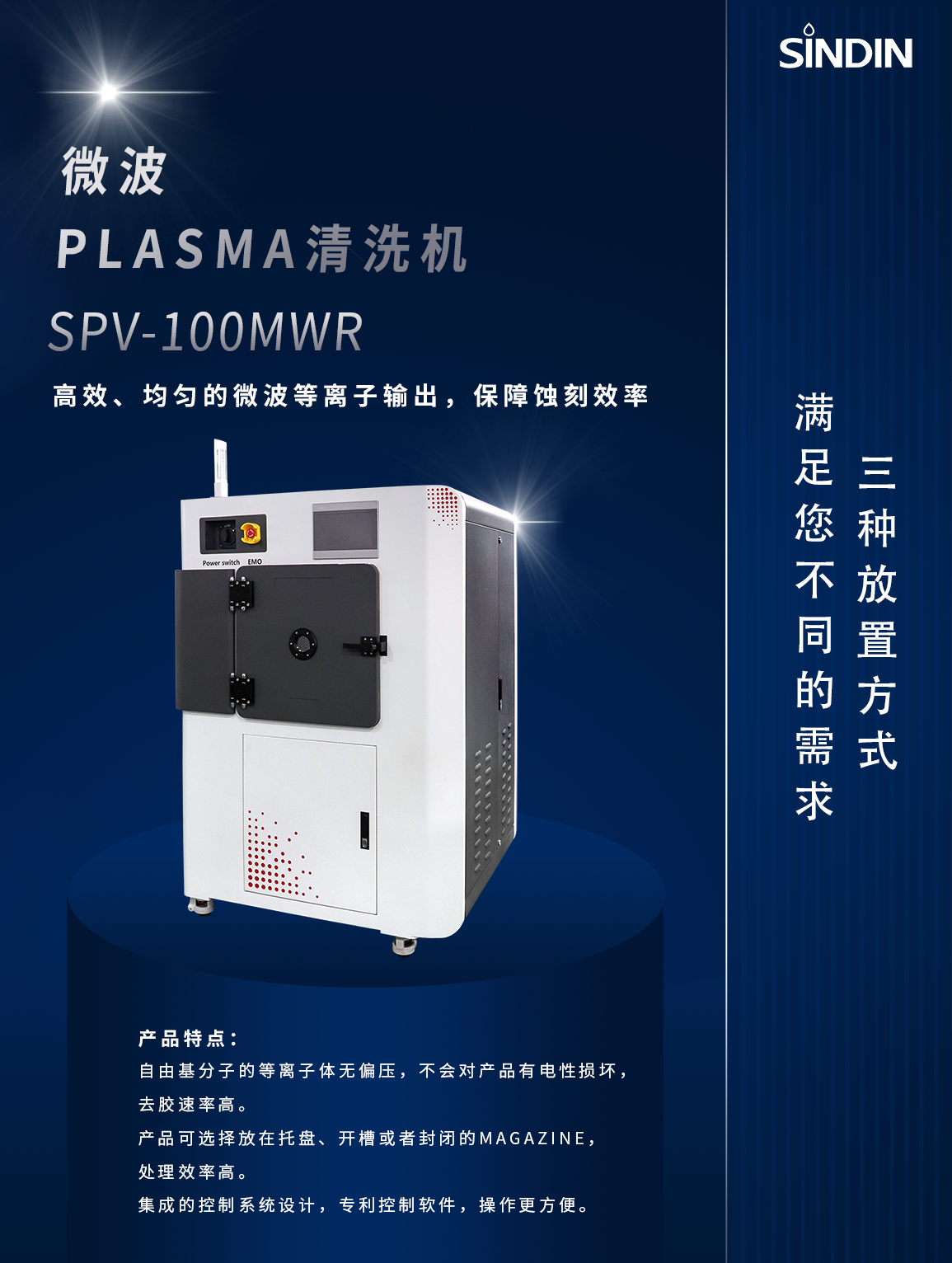
Contaminants in the packaging process can be treated by an ion cleaning machine, which is mainly used to remove material surface pollution by physical bombardment or chemical reaction of the active plasma on the material surface. However, due to technical factors such as treatment temperature and plasma density, RF plasma technology can no longer meet the technical requirements of advanced packaging, so it is more recommended to use microwave PLASMA cleaning technology~
Advantages of Microwave PLASMA Cleaner
Processing temperature lower than 45 ℃: avoid thermal damage to the chip
The plasma is not charged: it will not damage the precision circuit
04 Application of Microwave PLASMA in IC Packaging
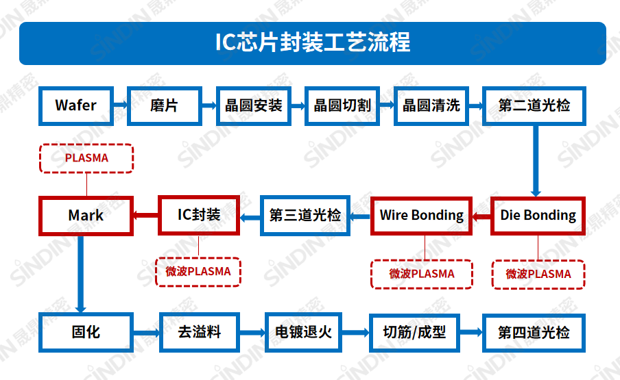
In the chip packaging process, microwave PLASMA cleaning machine is recommended for chip bonding/eutectic → lead welding → packaging → Mark and other process links, which can damage precision components without affecting the performance of the previous process and help effectively improve the chip packaging quality.
◾◾◾ Contact us for more process solutions ◾◾◾