


How to improve the reliability of microelectronic packaging?
With the continuous improvement of technology, the precision requirements of semiconductor IC process and packaging also increase. The photoresist remaining in the semiconductor chip manufacturing process will obviously affect the related process quality of the chip during the production process, thereby reducing the reliability of the chip and the product qualification rate. RF plasma technology cannot meet the needs of high-precision degumming, and it is easy to cause chip damage.Through the microwave plasma technology pioneered by Sindin in China, combined with the RF bias technology, the residues on the chip surface can be completely removed, thereby significantly improving the manufacturability, reliability and yield.
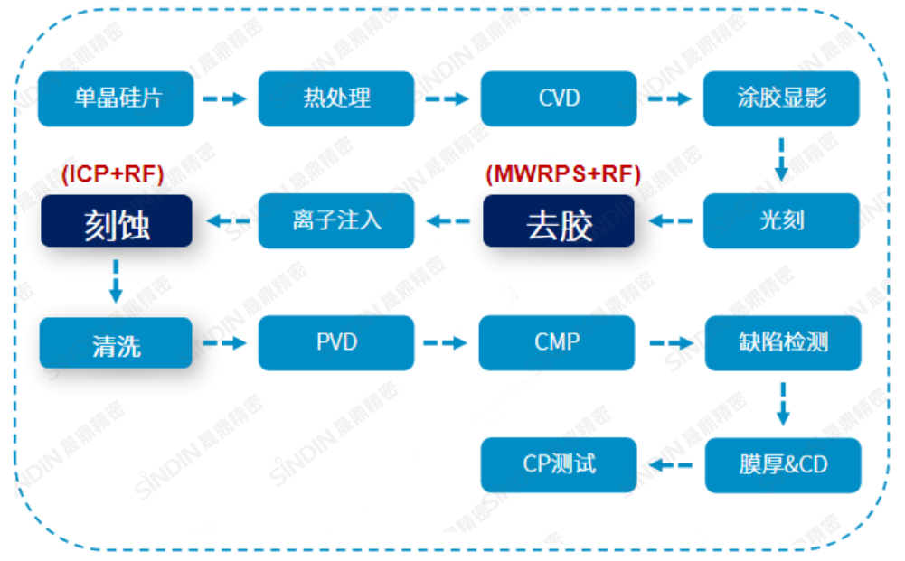
IC Manufacturing Process Flow Diagram
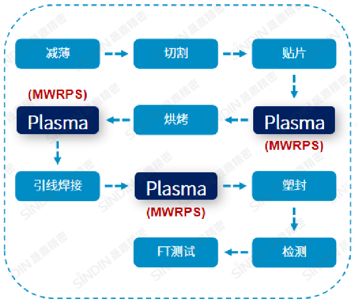
Chip packaging and testing process flow chart
What is microwave plasma?
When the gas is charged with enough energy, it will be ionized into plasma, such as electrons, atoms, radicals, radicals, etc. There are three kinds of common plasma power excitation frequencies, the excitation frequency of 40kHz is the ultrasonic plasma power supply, the 13.56MHZ is the radio frequency plasma power supply, and the 2.45GHZ plasma is the microwave plasma power supply.Microwave plasma is a gas that is excited by the high energy of microwaves to make it into microwave plasma.
Application of Microwave Plasma in Electronic Packaging
(1) FC package microwave plasma treatment:Flip-chip bonding (FC) refers to the connection of an integrated circuit chip with the active side down to a carrier or substrate. The interconnection between the chip and the substrate is realized by the bump structure on the chip and the bonding material on the substrate. This allows for both mechanical and electrical interconnection. At the same time, in order to improve the reliability of interconnection, underfill is added between the chip and the substrate. For high-density chips, flip-chip bonding has strong advantages in both cost and performance, and is the development trend of chip electrical interconnection.
In flip-chip packaging, after the solder balls of the flip-chip are connected to the pads of the substrate, and after cleaning the flux, it is still necessary to perform plasma cleaning between the chip and the substrate to remove organic contamination on the surface and perform surface reactivation. When underfilling, the fluidity of the glue can be greatly improved, so that the glue can be completely covered between the flip chip and the substrate,It does not cause voids, reduces the loss of fillers, improves the adhesion strength, reduces the generation of voids during heating, and improves product reliability and life.

(2) Wafer Plasma to remove residual glue:In the silver paste chip bonding process, the resin diffusion causes contamination or the organic solvent volatilizes during the curing process, and part of the volatiles will be deposited on the circuit surface, causing trace contamination on the surface of the chip, bonding or solder ring.In order to remove the contamination from organic solvents, microwave plasma cleaning is required after mounting and curing and before wire bonding.
(3) Pre-treatment of metal bonding:The quality of wire bonds has a decisive impact on the reliability of microelectronic devices. There must be no contaminants present in the bonding area. Microwave plasma cleaning can eliminate tiny dirt on the surface of the gold-plated layer and effectively improve the wettability of the welding surface.Enhance the mutual fusion of welding materials, thereby effectively enhancing the lead welding strength.
(4) Wafer surface activation:Microwave plasma cleaning can improve the hydrophilicity of the surface of the substrate material and increase the wetting performance, provide a good contact surface, make the eutectic solder and epoxy resin material have good fluidity on the surface, and can effectively prevent or reduce the generation of solder voids , to ensure highly reliable bonding and thermal conductivity.

Advantages of microwave plasma cleaners in packaging
The incoming process gas is excited by the microwave high-energy electromagnetic field, ionized to generate plasma, and directly acts on the surface of the product for cleaning, activation, degumming and etching.
.png)
Semiconductor industry application case
① Lead frame treatment:

②Fr4 plate etching:
.png)

