


From silicon wafer to battery wafer, see how Sindin plasma cleaning technology is used?
In the last issue, we shared how plasma can improve the reliability of solar photovoltaic panel packaging.
In this issue, we focus on the subdivision process to understand the application of plasma cleaning in solar photovoltaic cells!
Silicon-based photovoltaic cell process
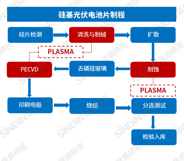
From wafers to batteries:
Take the current mainstream monocrystalline silicon PERC battery manufacturing process as an example, from the silicon wafer to the battery chip will probably go through: Wash and make velvet→Diffusion knotting→Etching & dephosphorization of silica glass→PECVD→
Printed electrode & Sintering→Sorting test / inspection into the database. And in cleaning, velvet, etching, PECVD and other links, can use Shengding plasma cleaning machine, let's look at the specific application.
Application of plasma cleaning technology in battery sheet technology
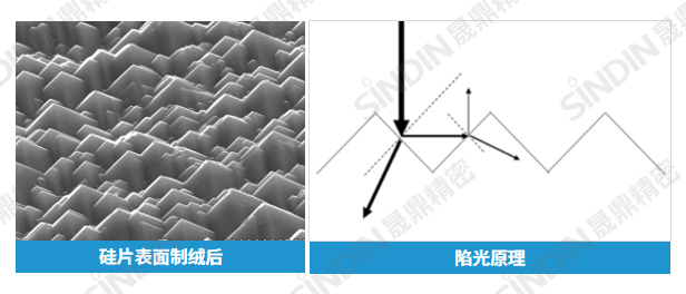
01 Wash and make velvet
In the process of cleaning and cashmere-making process, wet chemical cleaning is generally carried out with alkaline or acidic etching solution. The velvet-making effect is not only affected by many factors, but also the porous silicon structure is loose and unstable, and has a high surface recombination rate.
Treatment scheme of plasma cleaning machine:
By bombarding the battery surface with high-speed particles of plasma, the velvet surface can be treated in a more detailed and orderly manner, the surface structure can be more stable, and the production of composite centers can be reduced; at the same time, the fingerprint oil on the material surface can be removed, and the drying process of wet treatment can be reduced.
02 Etching & dephosphorization of silica glass
In the upper diffusion process, the photogenerated electrons collected at the front of the PN junction will spread along the edge and flow to the back of the PN junction, resulting in a short circuit.
Therefore, the doped silicon around the solar cell must be etched to remove the PN junction at the edge of the solar cell.
Plasma etching technology is usually used to complete this process.
The plasma can decompose the excess diffused phosphorus by particle purging, thus achieving the purpose of removing PSG.
03 PECVD
In order to reduce the surface reflection and improve the conversion efficiency of the battery, it is necessary to deposit a layer of silicon nitride antireflection film.
In industrial production, PECVD equipment is often used to prepare antireflection film, PECVD is plasma enhanced chemical vapor deposition, which uses low temperature plasma as energy source, the product is placed on the cathode of glow discharge at low pressure, the product is heated to a predetermined temperature by glow discharge, and then an appropriate amount of reaction gas SiH4 and NH3 are introduced. The gas goes through a series of chemical reactions and plasma reactions.
A solid film, namely silicon nitride film, is formed on the surface of the product.
Sindin plasma cleaning machine
It is suitable for the cleaning and activation of photovoltaic glass, battery, backplane, frame and other components, can be matched with direct injection or rotating gun head, and can be customized atmospheric plasma assembly line equipment.
It is suitable for the cleaning and activation of photovoltaic glass, battery, backplane and other components, and can be customized to wide-width linear plasma assembly line equipment.
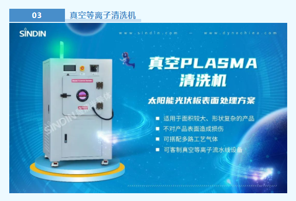
It is suitable for cleaning materials with large area and complex shape, can be matched with multi-channel process gas, and can be customized vacuum plasma assembly line equipment.

◾◾◾ For more solutions, contact us for more solutions ◾◾◾